Sources and Filters based on Superconducting Photonic Band Gap Structures
- True single frequency (no harmonics present)
- High Q, low phase noise resonators / filters
- Scalable to a wide range of frequencies
- Extremely stable and mechanically rigid
- Potential applications in spread spectrum modulation, Doppler radar, multichannel filter banks.
The concept of a photonic band gap is very similar in character to a number of other physical systems, most notably energy gaps in semiconductor band structures. The essential ingredients are a wave phenomenon and a regular lattice of wave scatters. In the case of semiconductors, the charged electrons are in a regular crystalline lattice of atoms (positive charge centers). With the proper electron density and periodicity of the lattice, one finds forbidden energy bands within which charges can not exist.
In a similar way, one may arrange for a periodic structure of dielectrics. The dielectric constants and the lattice can be chosen so as to create forbidden bands, or frequency ranges, in which electromagnetic waves cannot propagate, i.e., a photonic band gap.
To draw the analogy further, consider the effect of doping the semiconductor lattice with an impurity atom. Done properly (i.e., with the right impurity atom), one can create an energy state that exists within the forbidden energy band. In the same way, one may create an “impurity” or “defect” state in the photonic band gap by altering the size or dielectric constant of one of the lattice sites. An energy state will be localized about this impurity site, meaning the mode does not propagate through the lattice.
Once a “defect” mode is excited or energized, it will dissipate only in a few ways. If these avenues are somehow minimized, the excited mode will have a long lifetime and a very precise frequency, i.e., the defect mode in the photonic band gap is essentially a high Q “cavity”. It is this aspect of the photonic band gap that has attracted attention, as this provides a means of creating an ultrahigh precision frequency source for real world applications.
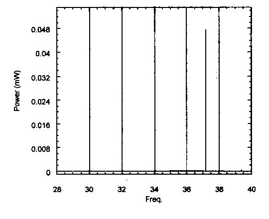
The PBG resonator is a true single frequency resonator, while all possible harmonics are present in the dielectric cavity resonators. Figure 3 shows typical transmission curve for the photonic band gap structure with a “defect”.
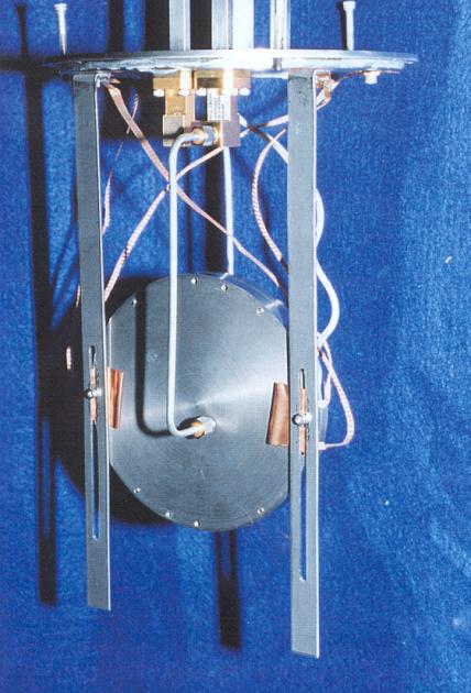
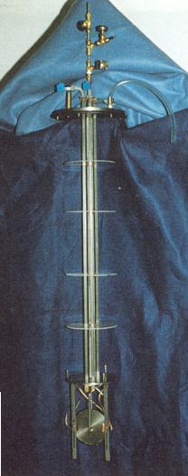
In principle, the concept of a photonic band gap can be applied in one, two or three dimensional dielectric lattices. Full three dimensional lattices can, and have been constructed. However, they are in practice very difficult to make, and the confinement of a defect mode depends upon the existence of a photonic band gap in all three dimensions. Two dimensional lattice, bounded above and below by conductive plates are much easier to realize in practice, and the theoretical calculations, while still difficult, are still easier to perform. The concepts and theory of PBG are completely scaleable to any desired operating frequency. Thus it is relatively easy to design a device for operation at any target frequency, and the same device can be operated over a small frequency range within the PBG by varying the size of the defect that creates the defect mode. The system in Figures 1 & 2 was designed to operate in the 35 GHz regime (K band), and the resultant device size was a little over 4 inches in diameter.
The energy loss mechanisms for a defect mode in a photonic band gap can be separated into three channels. One, the dielectric medium can be lossy. This can be characterized by a material property called the “loss tangent”. In choosing the dielectric medium to be used for the photonic band gap structure, one should select a material with a low loss tangent. Secondly, the defect mode, while localized, can extend to edge of the physical lattice where the mode can drive a propagating mode and allow energy to escape. This loss mechanism is referred to as confinement loss. The solution of this problem is simply to make the physical lattice large enough that the characteristic size of the mode, called the localization length, is many time smaller than the actual size of the lattice. Lastly, the bounding conductive surfaces above and below the two-dimensional structure have surface resistance which causes resistive heating, another loss mechanism. The solution to this problem is to select a highly conductive material (low surface resistance). Superconductors are obvious choices here.
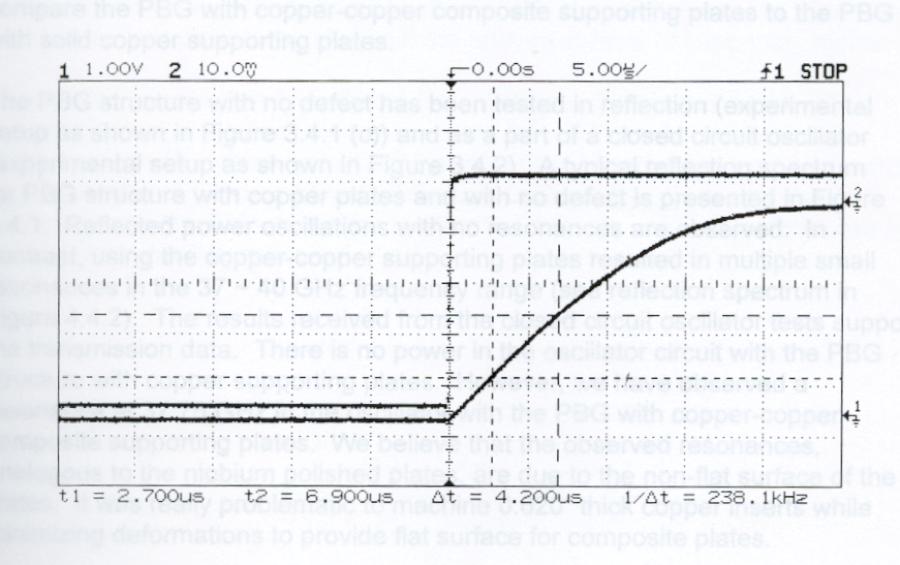
The observed Q for PBG resonator with copper plates at 77 K was in the range of 4000 ~ 12000. The PBG resonator with superconducting niobium plates operating at 4.2 K had the loaded Q values of 1.1×10⁶. The Q was evaluated through the time constant of energy decay stored in the resonator (see Figure 4). It is expected that the unloaded Q should be in the 1.1×10⁶ ~ 2.2×10⁶ range.