Microwave NDE
Tristan Technologies is involved with a number of instruments using microwave / millimeter wave techniques for the characterization of physical properties of various materials.
The instrument presented here is an example of a resonant cavity near field microwave system. Here, the energy from a resonant cavity is coupled outside the cavity via a small hole or a conductive wire, producing evanescent fields. The size of the hole or the wire is usually much smaller than the wavelength. The hole or wire size (not the wavelength) sets the spatial resolution for the imaging of materials. Depending upon the probe configuration, a spatial resolution on the order of l/1000 (where l is the resonant wavelength) can be achieved. The important parameters of the resonator are the resonant frequency (fo) and the quality factor (Q). A sample coupled into a resonator can change fo and / or Q. A change in Q is associated with surface resistance and dielectric losses. A shift in fo is caused by the material’s dielectric constant. Probes of this type are also called evanescent microwave probes (EMP). The main probe features include the following:
- high sensitivity to material characteristics
- high spatial resolution – fraction of a wavelength
- sensitive to surface properties of metals – surface resistance
- sensitive to structural and elctromagnetic properties of semiconducting materials and dielectric materials, including ceramics and composites
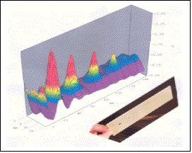
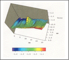
Figure 1. Shows the output from a scan over a 2.5 mm thick glass fiber composite plate, shown in the inset photograph. The plate contains 6 through holes of decreasing diameter going from left to right.
For metallic samples, surface defects and variations, perhaps indicating corrosion, can be revealed. For ceramic and composite samples, such structural defects as voids, delaminations or disbonds, porosity, and corrosion, produce local impedance changes, revealing their presence. A near field microwave instrument is only sensitive to surface and near-surface defects on metal samples; for dielectric samples, the thickness of the measured structures can be on the order of several centimeters, depending on the microwave wavelength and the scanning configuration.
For the data presented here, the sample under test was directly coupled to a 9 GHz high-Q resonant cavity through a several millimeter sized rectangular aperture, thus providing sub-wavelength resolution. In the microwave circuit, the resonant cavity was coupled so as to nearly match the impedance of the input circuit, so that only a minimal amount of power was reflected back. An advanced frequency modulation and feedback circuit, implemented in the present system, varied the frequency to lock the circuit on to the resonant frequency defined by the resonant cavity / sample combination.
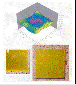
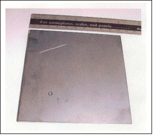
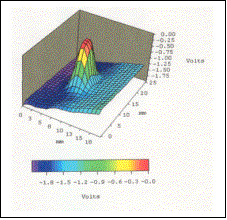
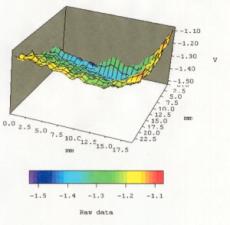
Figure 2. In this figure, the sample is a 6.4 mm thick, square, glass fiber composite plate. There are 9 drill markings on this plate, going from through holes to just shallow indentations. The photo in the lower right shows the plate from the back side, meaning that only the through holes mar the surface; some of the other markings are visible simply because the plate thickness is thinner below the markings. The markings are in a 3 x 3 array; note that there is no visible sign of the marking at the lower left. If the plate is turned over, this lower left marking is as shown (see the photo in the lower left); this marking is cone shaped with a 2.3 mm maximum depth and 9 mm diameter at the surface of the plate ¾ recall that the plate is 6.4 mm thick, so this marking is over 4 mm below the other surface of the plate. The output shown was produced when scanning the plate from the backside, over the marking shown in the lower left photo. If this marking represented a structural defect, its presence would be clearly revealed.
The variations in output shown in these figures correspond to changes in the reflected power — while using the feedback circuit to lock on to the resonant frequency of the cavity / sample grouping — as the aperture of the cavity is scanned over the sample. The changes in reflected power correspond to changes in the complex impedance of the cavity / sample combination; these impedance changes in turn reveal properties of the portion of sample directly below the aperture.
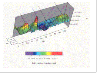
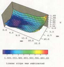
Figure 3: This is another example showing changes in reflected power caused by markings on a 2.3 mm thick fiberglass plate. The upper portion of the figure is a photo of the plate — moving from the left to the right side: 0.77 mm diameter blind hole; 0.77 mm diameter through hole; 0.61 mm diameter blind hole; 0.49 mm diameter blind hole (the blind holes extend approximately halfway through the plate.
4a 4b
4c 4d
4e 4f
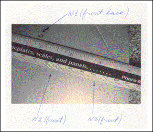
Figure 4: Scan of various markings in a 5 mm thick SiC ceramic plate: (a) is a photograph of the whole plate and (b) shows just the region of the 3 markings.Marking N1, in (b), is an annular groove, 4 mm OD X 2 mm ID X 2 mm deep. (c) shows the output of a scan directly over N1, clearly revealing this feature in a ceramic plate. (d) shows a scan of the same marking from the back side; this surface. In (b), N2 is a 1.5 mm diameter counterbore, less than 0.5 mm deep; a scan of this feature is shown in (e). N3 in (b) is 0.75 mm counterbore, less than 0.5 mm deep; a scan of this feature is shown in (f).
For non-destructive inspection / evaluation of dielectric samples, this near field microwave instrument has definite advantages over the other currently used techniques.
Mechanical testing: frequently destructive, only gives indirect information regarding the investigated structure.
Electron scanning microscopy: limited to surface characterization.
Conventional ultrasound: requires fluid coupling to the surface, which is time consuming and inconvenient.
X-ray characterization: not user friendly in the sense that the measurement must be shielded from the operator.
Thermal techniques: data interpretation difficult and confusing, especially for thick samples.
We feel this microwave near field, high-Q tool is a powerful NDE / NDI instrument. Design variations allow focusing on different applications. Tristan can provide a microwave near field scanner — including sensor (consisting of a resonant cavity at a specified frequency with various E and H field orientations outside the cavity), scan stage, computer control and data analysis ¾ for use in Non-Destructive Evaluation and Non-Destructive Inspection (NDE & NDI) applications, as well as physical properties characterization.
Contact us concerning your specific needs.